Research Areas
Micro-Electro-Mechanical-Systems (MEMS), Nano-Electro-Mechanical Systems (NEMS), Micro-Opto-Electo-Mecanical Systems (MOEMS), Bio-MEMS, Nano tech, Nanofabrication, Microfabrication
Projects
Fabry-Perot Interferometer (FPI)
This project consisted of design, simulation and fabrication of narrow-band dynamically tunable optical filter, working in the MWIR range (3-5 um). After testing, the filter is to be integrated with wide-band detector. Starting from the basic principles of the FPI, and analysis of the existing filter technology for use in MWIR. After considering all the advantages and failures, I came up with a unique design that included Bragg stacks as reflective material and SOI wafers as substrate. After researching the materials for the Bragg Sacks, I decided to use silicon oxide and germanium and simulated the behavior using MATLAB.
Using PECVD for the deposition of the silicon oxide and evaporator for the germanium, I deposited several varying Bragg stacks, and have compared their optical performance to simulations. The stress in all the layers was measured and conditions of deposition changed to minimize the stress.
In order to define a stable, robust and easy process for the filter, I ran a matrix of experiments using several etching methods to determine the optimal combination of steps (accounting for defects, surface roughness, yield). In the end, have achieved a process that is scalable to almost any wafer size, uses the least number of steps, and produces almost 100% yield. Ongoing are the mechanical and optical testing of the filter.
Fabrication and testing of a MEMS-based optical filter combined with a HgCdTe detector (pdf)
Lamellar Grating Project
As alternative to FPI filter, Lamellar grating is developed for Fourier filtering in the MWIR. I supervised several groups of students who designed various horizontal Lamellar grating filters, and send the designs out for fabrication. This was fabricated by MEMSCAP. Under my supervision, various designs have been tested.
I have developed vertical Lamellar filter, using IntelliSuite FEA to simulate its mechanical behavior. Fabrication work up to this point includes fabrication of vertical Lamellar filter on SOI wafer and development of chemical polishing to remove the roughness on the sidewalls after DRIE step.
Paper comming soon!!
NEMS switch based on carbon nano-fiber (CNF)
This project started from the concept of using carbon nano-fibers as mechanical elements in NEMS switch. From the initial phenomena, I have performed extensive FEA simulations to determine the mechanical properties of CNFs, such as Young’s modulus and Poisson’s ratio.
I have designed the device architecture and performed process simulations using MEMSPro software; the design is based on the fact that CNFs can grow vertically as single fibers from a metal catalyst dot. From the beginning of the process development, I have patterned arrays of catalyst dots using e-beam lithography to determine the effects of exposure and development times on the size of dots after metal deposition and lift-off. Miscelles were used to mimic the size of the e-beam deposited dots for testing arrays. Using the PECVD process, I determine the optimal plasma power, gas flow, and temperature to achieve the most advantageous CNF growth from catalyst dots. Then I analyzed the quality of resulting fibers using SEM, Raman and XPS spectroscopy. The base of the device was fabricated using a three-mask process; the masks were layout in LEdit. The rest of the device is made up of deposited layers of dielectrics and metals. A dry etching process was developed to pattern the device for CNF integration. Performed growth of CNFs on the devices.
I investigated and determined the solutions to multiple problems, such as grass formation, micromasking and selectivity problems. To work around incompatibility of PECVD process with previously deposited layers, I have attempted several process modifications.
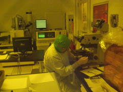
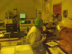
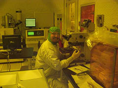
Part of my time at NASA, was devoted to maintaining and modifying several PECVD chambers and assisting group members in mask layout as well as fabrication and testing of their device.
Wafer-scale fabrication of a vertically-aligned NEMS switch based on carbon nanofibers (pdf)
EEL Project
I am a member of a group that is developing a device that uses microfluidics MEMS for energy generation. I helped with the initial design and made the layouts of the device that was fabricated at SMF. I also performed the fluidic testing.
Paper comming soon!!
Back Burner Projects
As every engineer, I have several personal interests in addition to the main projects. Whenever the money and time will come together, I will pursue these.